Intel never quite reached 4GHz with the Pentium 4. Despite being on a dedicated quest for gigahertz the company stopped short and the best we ever got was 3.8GHz. Within a year the clock (no pun intended) was reset and we were all running Core 2 Duos at under 3GHz. With each subsequent generation Intel inched those clock speeds higher, but preferred to gain performance through efficiency rather than frequency.
Today, Intel quietly finishes what it started nearly a decade ago. When running a single threaded application, the Core i7-2600K will power gate three of its four cores and turbo the fourth core as high as 3.8GHz. Even with two cores active, the 32nm chip can run them both up to 3.7GHz. The only thing keeping us from 4GHz is a lack of competition to be honest. Relying on single-click motherboard auto-overclocking alone, the 2600K is easily at 4.4GHz. For those of you who want more, 4.6-4.8GHz is within reason. All on air, without any exotic cooling.
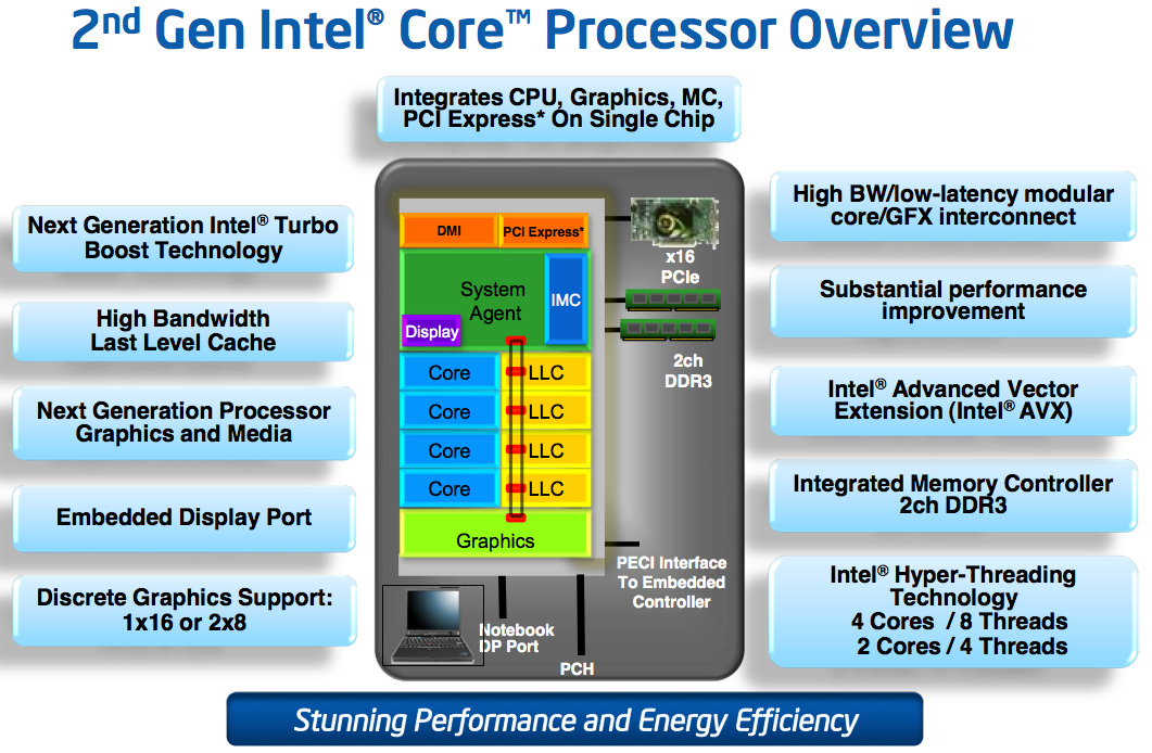
Unlike Lynnfield, Sandy Bridge isn’t just about turbo (although Sandy Bridge’s turbo modes are quite awesome). Architecturally it’s the biggest change we’ve seen since Conroe, although looking at a high level block diagram you wouldn’t be able to tell. Architecture width hasn’t changed, but internally SNB features a complete redesign of the Out of Order execution engine, a more efficient front end (courtesy of the decoded µop cache) and a very high bandwidth ring bus. The L3 cache is also lower and the memory controller is much faster. I’ve gone through the architectural improvements in detail here. The end result is better performance all around. For the same money as you would’ve spent last year, you can expect anywhere from 10-50% more performance in existing applications and games from Sandy Bridge.
I mentioned Lynnfield because the performance mainstream quad-core segment hasn’t seen an update from Intel since its introduction in 2009. Sandy Bridge is here to fix that. The architecture will be available, at least initially, in both dual and quad-core flavors for mobile and desktop (our full look at mobile Sandy Bridge is here. By the end of the year we’ll have a six core version as well for the high-end desktop market, not to mention countless Xeon branded SKUs for servers.

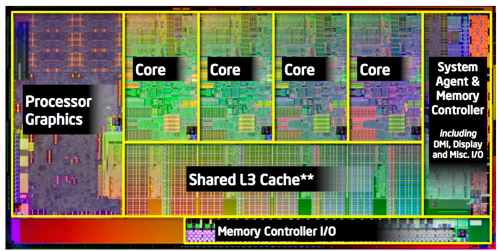
The quad-core desktop Sandy Bridge die clocks in at 995 million transistors. We’ll have to wait for Ivy Bridge to break a billion in the mainstream. Encompassed within that transistor count are 114 million transistors dedicated to what Intel now calls Processor Graphics. Internally it’s referred to as the Gen 6.0 Processor Graphics Controller or GT for short. This is a DX10 graphics core that shares little in common with its predecessor. Like the SNB CPU architecture, the GT core architecture has been revamped and optimized to increase IPC. As we mentioned in our Sandy Bridge Preview article, Intel’s new integrated graphics is enough to make $40-$50 discrete GPUs redundant. For the first time since the i740, Intel is taking 3D graphics performance seriously.
| CPU Specification Comparison |
| CPU | Manufacturing Process | Cores | Transistor Count | Die Size |
| AMD Thuban 6C | 45nm | 6 | 904M | 346mm2 |
| AMD Deneb 4C | 45nm | 4 | 758M | 258mm2 |
| Intel Gulftown 6C | 32nm | 6 | 1.17B | 240mm2 |
| Intel Nehalem/Bloomfield 4C | 45nm | 4 | 731M | 263mm2 |
| Intel Sandy Bridge 4C | 32nm | 4 | 995M | 216mm2 |
| Intel Lynnfield 4C | 45nm | 4 | 774M | 296mm2 |
| Intel Clarkdale 2C | 32nm | 2 | 384M | 81mm2 |
| Intel Sandy Bridge 2C (GT1) | 32nm | 2 | 504M | 131mm2 |
| Intel Sandy Bridge 2C (GT2) | 32nm | 2 | 624M | 149mm2 |
It’s not all about hardware either. Game testing and driver validation actually has real money behind it at Intel. We’ll see how this progresses over time, but graphics at Intel today very different than it has ever been.
Despite the heavy spending on an on-die GPU, the focus of Sandy Bridge is still improving CPU performance: each core requires 55 million transistors. A complete quad-core Sandy Bridge die measures 216mm2, only 2mm2 larger than the old Core 2 Quad 9000 series (but much, much faster).
As a concession to advancements in GPU computing rather than build SNB’s GPU into a general purpose compute monster Intel outfitted the chip with a small amount of fixed function hardware to enable hardware video transcoding. The marketing folks at Intel call this Quick Sync technology. And for the first time I’ll say that the marketing name doesn’t do the technology justice: Quick Sync puts all previous attempts at GPU accelerated video transcoding to shame. It’s that fast.

There’s also the overclocking controversy. Sandy Bridge is all about integration and thus the clock generator has been moved off of the motherboard and on to the chipset, where its frequency is almost completely locked. BCLK overclocking is dead. Thankfully for some of the chips we care about, Intel will offer fully unlocked versions for the enthusiast community. And these are likely the ones you’ll want to buy. Here’s a preview of what’s to come:
The lower end chips are fully locked. We had difficulty recommending most of the Clarkdale lineup and I wouldn’t be surprised if we have that same problem going forward at the very low-end of the SNB family. AMD will be free to compete for marketshare down there just as it is today.

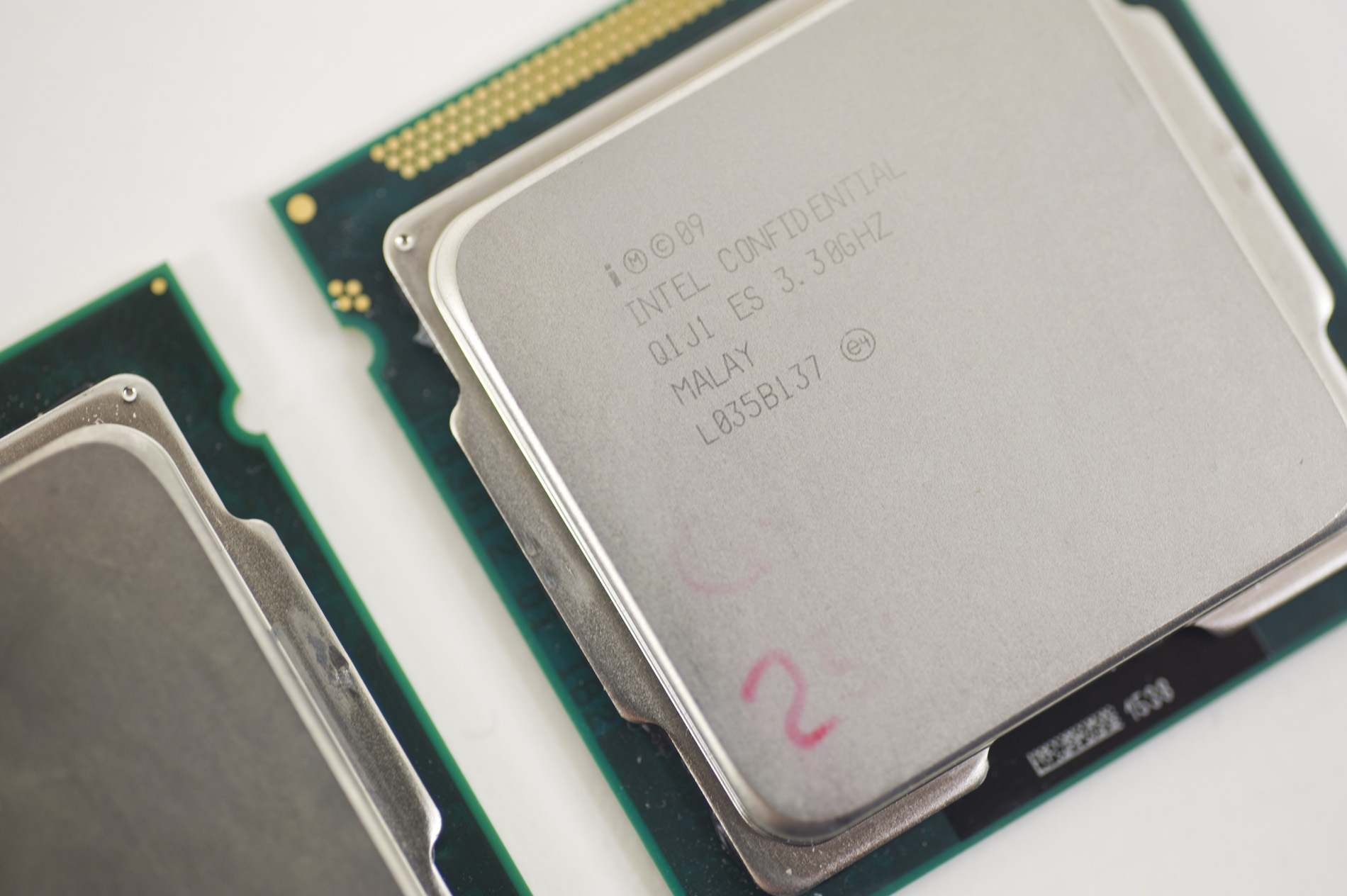
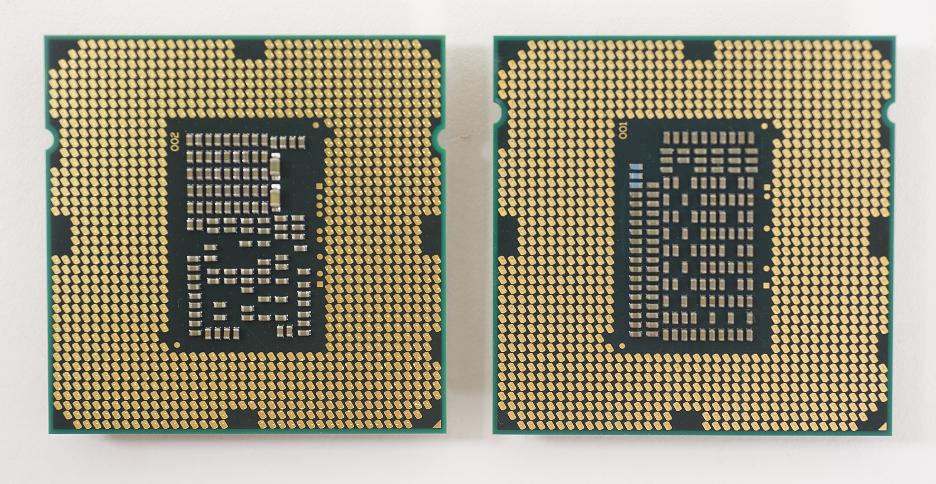
With the CPU comes a new platform as well. In order to maintain its healthy profit margins Intel breaks backwards compatibility (and thus avoids validation) with existing LGA-1156 motherboards, Sandy Bridge requires a new LGA-1155 motherboard equipped with a 6-series chipset. You can re-use your old heatsinks however.

Clarkdale (left) vs. Sandy Bridge (right)
The new chipset brings 6Gbps SATA support (2 ports) but still no native USB 3.0. That’ll be a 2012 thing it seems.
Refer To : http://www.anandtech.com